To help us provide you with free impartial advice, we may earn a commission if you buy through links on our site. Learn more

If you’ve read a laptop or smartphone review that’s of even a mildly technical nature, you may have come across the term “manufacturing process”. You might see CPU specifications mentioning the term 3nm or 5nm and – if you’re old enough like me – you might even remember when CPUs had 14nm and higher in the specifications.
It’s a term that refers to the smallest size at which a CPU factory, or fab, can etch out the components from a silicon wafer that go to make up your CPU – the transistors, in other words. And for Intel, the next big milestone along the way is 18A – or what one would generally call “1.8nm”.
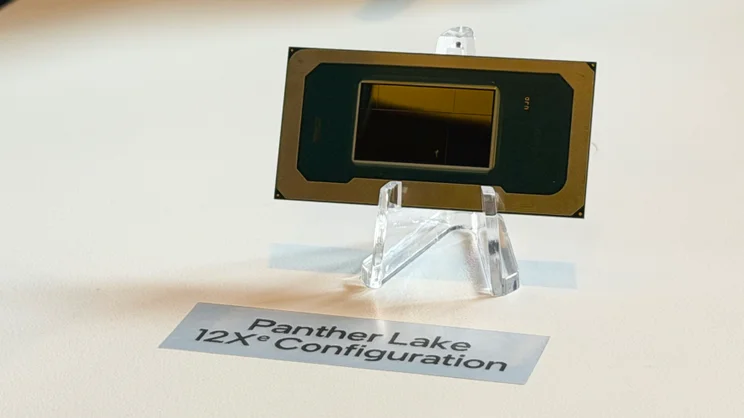
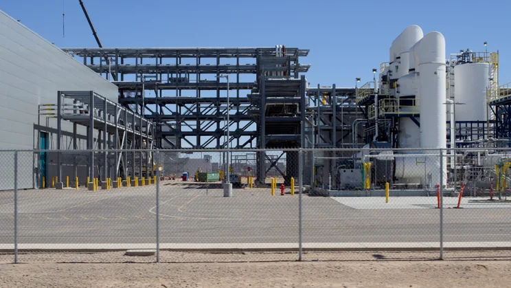
I was recently lucky enough to participate in a tour of Intel’s latest 18A factory in Phoenix, Arizona, as part of the Intel Technology Tour 2025 event – where the company launched its next-generation Panther Lake laptop chip.
This is one of two facilities where the chip giant will be making CPUs based on the new technology, and it’s a huge investment for the company. Each of the fabs represents a massive $20 to $25 billion investment and four years of construction involving thousands of workers. And you really get a sense of the huge size of the facilities required to produce these chips when you get the chance to look inside.
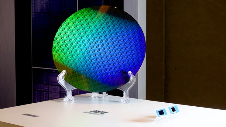
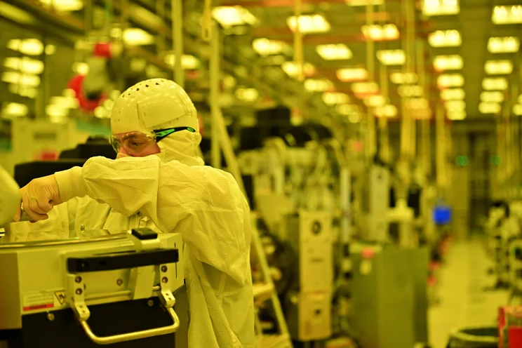
Fab 52, where Intel is putting the new 18A technology into production, is just one of multiple facilities on the one square mile site – it took our tour bus nearly half an hour to drive around the perimeter. Even walking through one part of it, from Fab 62 to the brand spanking new Fab 52 and then back again, clothed from head-to-toe in my white cotton, clean-room “bunny suit”, took minutes.
Greater efficiency, better battery life?
So why the big investment? The reason chip manufacturers like Intel and rivals such as TSMC and Samsung care about shrinking the size of the manufacturing process is simple: they can squeeze more capabilities into ever smaller packages, and a by-product of those smaller components is usually improved efficiency.
In fact, by Intel’s estimation, the efficiency gain of going to 1.8nm CPUs from Intel’s 3nm CPUs means an increase in performance per Watt greater than 15%, while the chip density is up by 1.3x. Perhaps more important than this, however, is that the foundation block of all silicon chips – the transistor – has had a bit of a redesign.
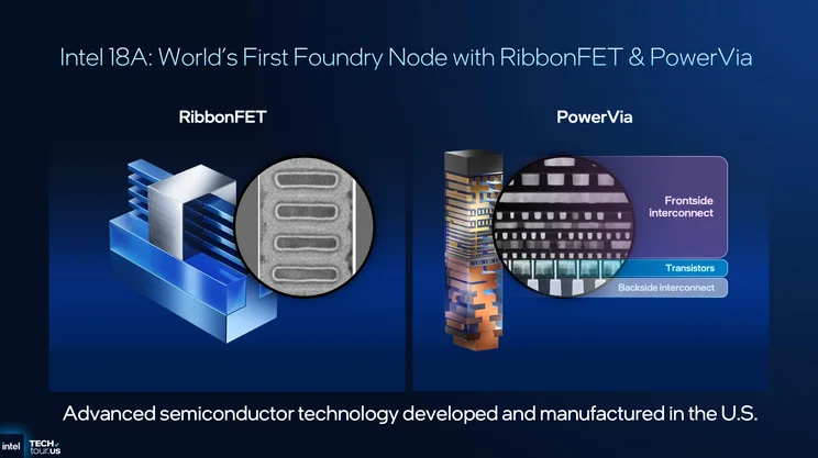
The new RibbonFET transistor is what’s known as a “gate all-around” design: it limits leakage current allows for better control and allows engineers to scale the process down even further. More important than that, however, is that 18A uses a new technology called PowerVIA, where the “wiring” connecting these transistors to a power source has been moved from the front of the wafer to the rear. This frees up space on the front for the signal lines to spread out, reducing interference and making room to squeeze in even more transistors.
One of the reasons we’ve seen battery life improve in smartphones and laptops over the past few years is that CPU manufacturing technology has progressed so fast. It wasn’t too long ago that 14nm chips were commonplace – in Intel’s Broadwell CPUs back in 2014 – this manufacturing process is a whopping seven times smaller than that.
The reason we haven’t seen it progress maybe as fast as we’d have liked, though, is that software and product development always wants to take full advantage of the extra power available to it. And don’t forget that the other components in a system like a laptop or smartphone won’t necessarily be advancing at the same rate when it comes to power efficiency. Screens, cameras, speakers, microphones and so on all consume power, too.
Even within the same chip, not every part is built using the same technology. Intel’s upcoming Panther Lake mobile chip, to use a contemporary example, is made up of a series of “chiplets”: the portion of the chip built with Intel 18A comprises the CPU, the ISP (image signal processor), the new NPU 5 and the media and display engines; the GPU, meanwhile, is built on Intel’s 3nm manufacturing process.
So you can see that even with billions of dollars of investment, that may not lead to the huge gains in battery life that you might expect, especially not with this first generation of 18A chips. The gains in power efficiency and compute density are likely to benefit users of Intel’s new Cloudwater Forest server chips more effectively, where the CPUs are packed together and make up much more, proportionally, of a datacentre’s requirements.
When will 18A make it into products?
Either way, we will find out how big or small an impact 18A will have on the performance and battery life of the products it is featured in very soon. Intel’s factories are already producing Panther Lake chips in high volume and the first laptops with Panther Lake chips are set to launch at CES 2026.
With both TSMC, who supply Apple, Qualcomm and AMD, and Samsung, also set to launch 2nm class products at around the same time, the next year looks like it could be an interesting one in the world of chip manufacturing.